Electrical Excitation of Plasmons in Metallic Nanostructures
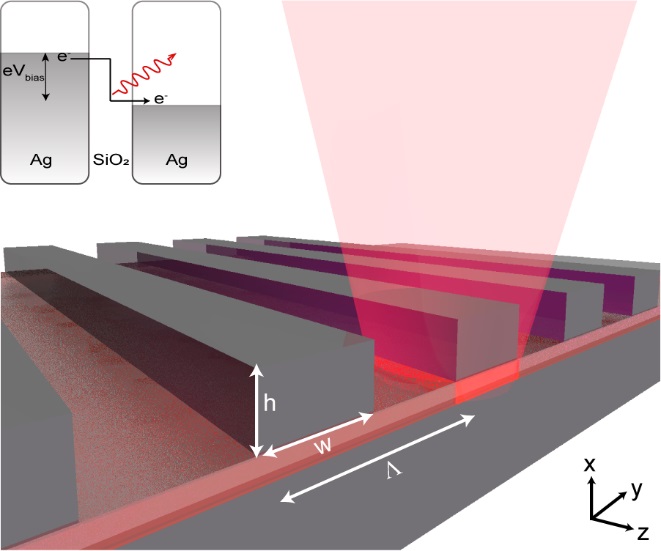 Representative image showing optical emission from MIM tunnel junctions (See [1] for further details)
Surface plasmons (SP), the collective oscillations of electrons on a metal-dielectric interface, have enabled squeezing of light into nanoscale dimensions leading to unparalleled control and manipulation of information at length scales much smaller than the wavelength of light. These electromagnetic waves propagate along metal-dielectric interfaces and can be guided by metallic nanostructures beyond the diffraction limit. Plasmonic circuits, therefore, possess both the capacity of photonics and miniaturization of electronics, paving the way for the development of nanoscale optoelectronic circuitry for computing and sensing applications. Electrical excitation of surface plasmons through the process of inelastic electron tunneling (IET) has gained immense popularity in recent years due to its unique potential to create ultra-compact photon and SP sources. In our group, we are investigating ways to improve the efficiencies of surface plasmon generation from electrically excited metal-insulator-metal tunnel junctions for the realization of ultra-compact on-chip optical sources which are readily integrable with existing CMOS technologies for practical on-chip applications. Our recent work in this direction is highlighted below –
Enhanced light emission from electrically excited nano-strip MIM tunnel junctions
We explored the light generation through inelastic electron tunneling in a periodic Ag-SiO2-Ag tunnel junction. We investigated the complex interplay between the optical modes of the tunnel junction, the antenna modes, and the lattice resonance arising from the periodicity of the structure. Our analysis revealed an enhanced radiative efficiency from hybridization of the optical gap plasmon mode and the lattice resonance, with an enhancement of ~30% as compared to the structure without the lattice resonance. This improvement is due to the direct out-coupling of the propagating SPs to free-space photons mediated by the grating. The emitted spectrum can be tuned to the desired wavelength range, from visible to near IR, by designing the geometrical and material parameters of the device accordingly for on-chip photonic and plasmonic applications.
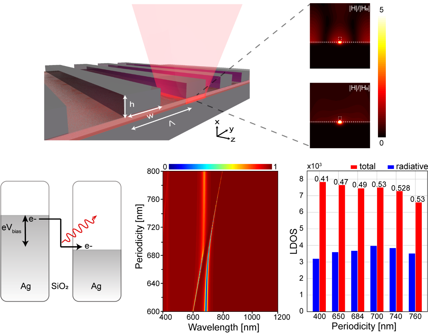
Figure 1: Optimization of MIM tunnel junction geometry to improve the radiative emission of electrically excited plasmons. Further details can be found reference [1]..
Reference
- Saurabh Kishen, Jinal Kiran Tapar and Naresh Kumar Emani. Enhanced light emission from gap plasmons in nano-strip MIM tunnel junctions. Journal of Optics, 22, 095006 (2020). [ doi | pdf ]